
Last month I wrote about how LLM inference got dramatically faster without any new hardware. Better cache quantization, multi-token prediction, smarter kernels. Software squeezing more out of the same GPUs.
This post is about the other layer: hardware. The ideas emerging in this layer are so different that the distinction between chip and model starts to dissolve.
Two companies made news that pulled me down this rabbit hole. Taalas, a 24-person team that literally hard-wired Llama 3.1 8B into a piece of silicon. And Etched, which came out of stealth on June 30 with working transformer ASICs, $800 million raised, and over a billion dollars in signed customer contracts.
Both are targeting the biggest bottleneck LLMs currently have. To understand why they exist, you need to understand what that bottleneck actually is.
The Next Token Tax
At its core, text generation in an LLM boils down to two main steps. First, the prefill stage reads the entire input prompt in parallel, a highly efficient, compute-bound operation. Second, the decode loop takes over to generate new text token by token. Because this loop must constantly access memory until a stop token is triggered, it turns the process into a notoriously memory-bound bottleneck.
This means that a GPU generating text spends most of its time not computing. It spends it waiting for memory.
Every single token a model produces requires reading essentially all of the model's weights from memory. For an 8B model at 16-bit precision, that is 16 gigabytes of data moved per forward pass. An H200 has around 4.8 TB/s of memory bandwidth, so even with perfect efficiency you hit a hard ceiling of roughly 300 tokens per second per user, and in practice you get far less. The compute units sit idle while weights stream in from HBM stacks bolted next to the die.
The entire modern inference stack is a workaround for this. High-bandwidth memory, advanced packaging, batching dozens of users together to amortize each weight read, liquid cooling to handle the power draw of shoveling terabytes around. It works, but it is expensive and inefficient.
Taalas: The Model as a Cartridge
Taalas, founded by Ljubisa Bajic (previously CEO of Tenstorrent), decided the memory-versus-compute divide is not a law of physics. It's a habit.
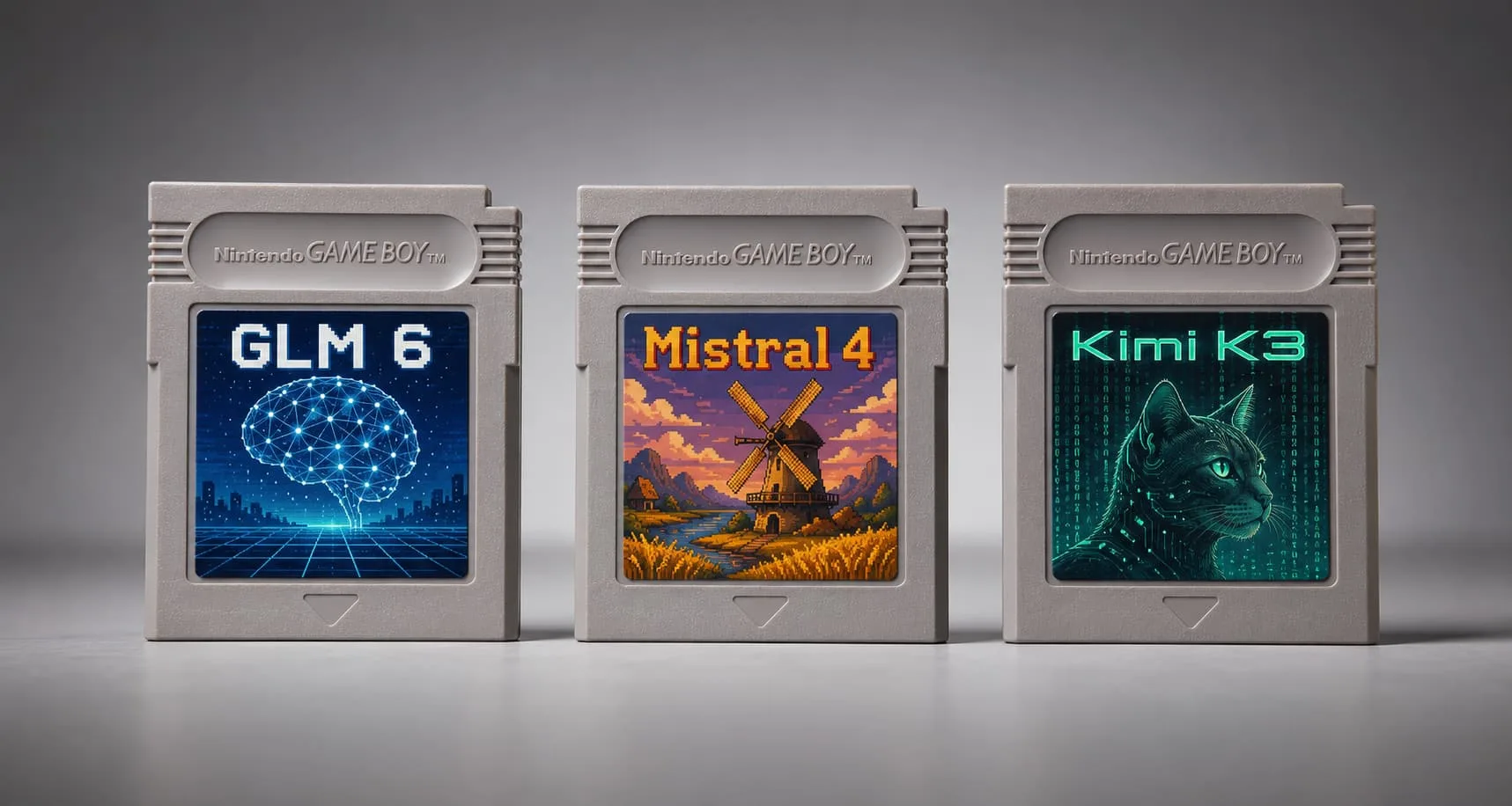
Their first chip, the HC1, is an 815 mm² die on TSMC's N6 process with Llama 3.1 8B baked directly into it. The weights don't live in DRAM or SRAM. They live in mask ROM, the same technology that stored Super Mario on an NES cartridge. Mask ROM reaches near-DRAM density but sits on the logic die itself, right next to the compute. The weights never travel anywhere. SRAM is reserved for the things that actually change at runtime: the KV cache and LoRA adapters.
The numbers this produces are hard to believe until you remember there is no memory wall left to hit. 17,000 tokens per second, per user. Not batched aggregate throughput, per user. That is roughly 10x faster than Groq and Cerebras, on a single air-cooled board that Taalas claims costs 20x less to build and draws 10x less power than the GPU baseline.
The manufacturing trick is what makes this a business rather than a stunt. The chip is a structured ASIC: around 100 layers are prefabricated and identical for every model, and only two metal layers get customized per model. A new model goes from checkpoint file to working silicon in about two months. Bajic describes the goal as a hardware compiler, and that's the right frame. You compile a model to CUDA today. Taalas compiles it to silicon.
The catch is real, though. The HC1 uses an aggressive custom 3-bit format with 6-bit weights sprinkled where needed, and Taalas admits it degrades quality versus GPU inference. Their second-generation platform moves to standard 4-bit floats. And obviously you cannot update a hard-wired model. You can fine-tune via LoRA and you can change the context, but the base weights are as fixed as the plastic they're wrapped in. A new model means a new chip.
They built all of this with 24 people and $30 million of the $219 million they raised. In an industry where the default hardware startup burns half a billion before first silicon, that stands out.
Update, August 2026: AMD announced it is acquiring Taalas, with plans to fold the hard-wired chips into its Helios racks alongside Instinct GPUs. I have mixed feelings about this. The team built something remarkable with 24 people, and they deserve the exit. But I was rooting for Taalas as an independent third pole in a market that is otherwise a duopoly, and after Nvidia's $20 billion Groq deal earlier this year, every interesting inference architecture now seems to end up inside one of the two incumbents. The consolation: Lisa Su is right that there is no one-size-fits-all chip, and if AMD actually ships hard-wired model cartridges at scale, the idea wins even if the startup doesn't stay independent. Still, I would have liked to see what they did on their own.
Etched: One Architecture, Not One Model
Etched sits one step down the specialization ladder. Instead of freezing a specific model into silicon, they froze an architecture: the transformer.
The bet looked insane when they made it in 2022, before ChatGPT, when betting a whole company on one neural network architecture seemed like a good way to get killed by a research paper. Four years later the transformer is still the substrate of everything, and the bet is paying off. Their announcement in June 2026 included first-pass working silicon on TSMC's N4P process, a rack-scale system handling both prefill and decode, and customers already running DeepSeek, Qwen, and Llama on it.
The scale is a different league from Taalas: 400+ employees pulled from NVIDIA, Broadcom, and Google's TPU team, a $5 billion valuation from their December round, and a stated path to gigawatt-scale production in 2027. Where Taalas is a precision instrument, Etched is building the thing that wants to replace the H100 in actual data centers near-term.
The trade-off between the two approaches is clean. Etched can run any transformer, so a new model release is a software update. Taalas runs exactly one model, but with weights physically adjacent to compute, nothing that keeps its flexibility can match its speed. Every rung of the ladder from general to specific buys you roughly an order of magnitude: GPU to architecture-specific ASIC, ASIC to model-specific silicon.
The Part That Actually Excites Me
Everything above is data center news, for now. Here is why I think it ends up in your basement.
Remove HBM, advanced packaging, liquid cooling, and high-speed interconnects from an inference system and what remains is a chip on a cheap board with a heatsink. That is not a data center component. That is a consumer electronics component. The HC1 board in Taalas's announcement photos looks less like a DGX node and more like something you'd slot next to the NAS in your closet.
Follow the roadmap a few years out. Taalas plans a frontier-class LLM on their second-generation silicon by winter. Suppose the economics hold as they scale: a model at, say, 70B parameters, hard-wired, air-cooled, drawing about as much power as a gaming console under load. At 20x lower build cost than GPU systems, that lands in the price range of a decent graphics card. You would buy intelligence the way you used to buy games: a specific model, on a physical card, that is entirely yours.
I've written before about local-first assistants and why I want models close to my own data. The blocker was never desire, it was that running a serious model at home means a €15,000 GPU rig that doubles as a space heater and still produces 30 tokens per second. A hard-wired model inverts every one of those constraints. Thousands of tokens per second means an agent that reads a full document and answers before your finger leaves the mouse button. No API bill, no rate limits, no conversation logs on someone else's infrastructure.
The frozen-weights problem bothers me less than it should. My daily use has quietly stopped depending on having the newest model. A good 2026-class model with LoRA fine-tuning, tool access, and my own documents in context covers most of what I actually do. The weights being a year old matters less when the model can search, and everything personal lives in the context anyway, which stays fully updatable. The cartridge is fixed. The save file is yours.
Not a Bigger Room
Bajic opens the Taalas announcement with ENIAC, and the analogy earns its place. ENIAC, the first of its kind, filled a room, drank 150 kilowatts, and got humanity exactly one computer. The transistor didn't make ENIAC better. It made ENIAC irrelevant, by making computing small and cheap enough to be boring.
Today's inference infrastructure has strong ENIAC energy. Gigawatt campuses, dedicated power plants, cooling towers. The industry's answer to demand has been to build the room bigger. And we are hearing the same arguments that were made against personal computers back in the 80s: who would ever need one at home, and why would you want it there.
Taalas, Etched and other startups are betting on the transistor moment for AI. That the future of AI is not a bigger room but a smaller chip, produced by the million, cheap enough that nobody thinks about it. With Taalas now heading into AMD, that bet increasingly plays out inside the incumbents rather than against them. First silicon is a long way from a product line, aggressive quantization has burned people before, and NVIDIA has kept winning so far. But for the first time, the path from "AI lives in a data center" to "AI lives in a slot in my home server" has actual working hardware on it.
I really hope we get there. Realistically it will still take 5 to 10 years, especially to scale these technologies. But if we do, intelligence will be truly ubiquitous.
Links
- The path to ubiquitous AI: Ljubisa Bajic's announcement of the hard-wired Llama
- Turing Post on Taalas: the best technical breakdown of the structured-ASIC approach and its trade-offs
- Etched emerges from stealth: working silicon, $800M raised, $1B+ in contracts
- How LLMs Got Faster Without New Hardware: my earlier post on the software side of the same fight